The short version
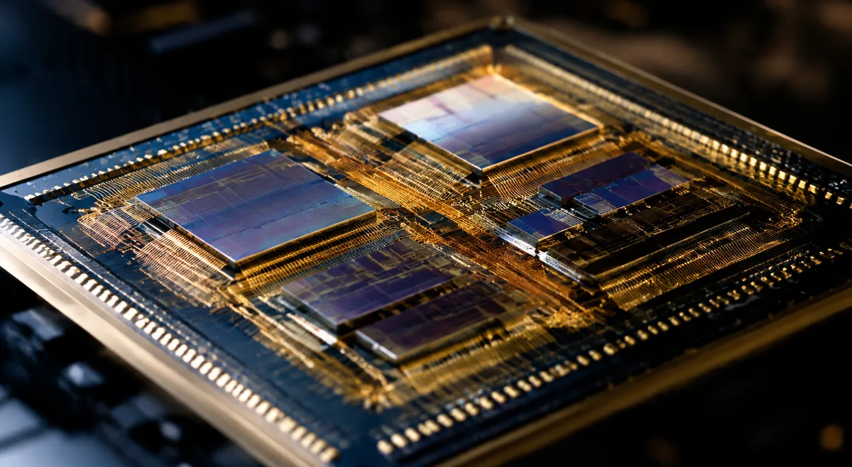
If you buy chips, you probably watch wafer capacity. For the next two years, you should be watching packaging capacity instead. On October 8, 2026, GlobalFoundries announced a manufacturing agreement with TSMC to build a US-based supply of silicon interposers for TSMC's CoWoS advanced-packaging ecosystem — a five-year deal valued at $2 billion, with production ramping at GF's Malta, New York fab in the first half of 2028. The interposer is a thin layer of silicon that sits between a chip and its package, carrying the wiring that lets a GPU talk to high-bandwidth memory at speed. It is the least glamorous part of an AI accelerator — and repeatedly among the tightest constraints on how many accelerators actually ship.
What was actually announced — and what wasn't
Tier the evidence before drawing conclusions. **Company announcement (GlobalFoundries, October 8, 2026):** GF will provide manufacturing services to TSMC and expand capacity at its Malta, New York plant to create what it calls the first US production site for silicon interposers, supporting embedded deep-trench capacitor technology. The agreement's initial term is five years, with a framework to expand as customer demand grows. Ed Kaste, GF senior vice president of the CMOS business, described 'a secure, scalable source of essential advanced-packaging elements' for AI and high-performance computing. Mass-production ramp is targeted for the first half of 2028. **Media report (Seoul Economic Daily via Yahoo Finance, October 9–12, 2026):** TSMC will source interposers from the US under a $2 billion five-year contract, shifting a component that has mainly been produced in Taiwan until now. The same reporting notes the two companies sued each other over patents in 2019 and settled within about two months — a detail that makes today's cooperation more striking, not less. **Media analysis (Chinese tech and financial coverage, October 8–9, 2026):** Coverage adds context — the CoWoS-S/R/L technology branches, the OSAT ecosystem, and the broader reshaping of the advanced-packaging landscape — all treated here as analysis, not confirmed figures. **What is not in the sources:** any statement from TSMC itself about the deal, any confirmed split of interposer volume between Taiwan and the US, and any commitment that the 2028 ramp date is guaranteed rather than planned. The deal is real; the timeline is a plan.
Why the interposer is the bottleneck
Buyers understand wafer shortages instinctively: no wafers, no chips. The interposer bottleneck works differently, and it matters more for AI hardware. An AI accelerator is not one chip. It is several — a GPU die, multiple HBM stacks, sometimes I/O or networking dies — wired together on a single interposer through silicon vias and dense routing. TSMC's CoWoS (chip-on-wafer-on-substrate) is the packaging technology that makes this possible, and it is the packaging inside Nvidia's AI accelerators. When interposer capacity falls short, finished accelerators don't ship — even if every die is ready. CoWoS capacity has lagged surging AI chip demand and become a major supply bottleneck (Seoul Economic Daily, 12 Oct 2026). This is why the GF deal matters beyond its dollar figure. TSMC is not outsourcing its crown jewels — interposer fabrication is built on mature-process platforms (deep-silicon etch, high-density routing), the kind of specialty-process work GF already does well. What TSMC is buying is *elasticity*: external capacity it can in principle dial up without building another fab. And the "first US site" label matters for a different reason — tariff resilience. An interposer made in Malta, New York is an interposer that doesn't cross the Pacific — a resilience point whose real value depends on how trade policy lands.
The timeline: three planning coordinates for 2026–2028
Forecasts disagree on details, but they agree on direction. Here are the three dates buyers should plan around — each from a named source, each with its own unit of measurement (don't mix them): | Period | What the forecast says | Source and caliber | What it means for buyers | |---|---|---|---| | 2026 | CoWoS supply/demand gap holds at ~20% | Counterpoint Research — analyst estimate | The bottleneck is still binding now. Lead times on packaged AI components stay long; plan as if nothing has changed yet | | 2027 | Gap narrows to ~10% as TSMC's internal capacity expands toward 185,000 wafers/month | Counterpoint — analyst estimate; TrendForce separately projects ~60%+ capacity expansion | Relief is scheduled, not delivered. Treat 2027 quotes "subject to capacity" as carrying real optionality | | H1 2028 | GF's Malta interposer capacity begins volume ramp | GlobalFoundries — company plan, not guarantee | External US capacity is planned to come online, on GF's schedule. The question for buyers is whether it lands before or after demand catches up again | Two cautions from our reporting discipline. First, the gap figures (percentages) and the capacity figures (wafers per month) are different metrics from different analysts — Counterpoint's gap and Economic Daily News' estimate (via TrendForce News) of 120,000–140,000 wafers/month for 2026 — plus 50,000–60,000 from OSAT partners — describe the same market in incompatible units, so don't combine them into a single number. Second, 2028 is when GF *plans* to ramp; plans slip. The responsible read: the bottleneck has a scheduled end date, but no confirmed one.
A buyer's packaging-capacity diligence checklist
Wafer-capacity questions are second nature to procurement teams. Packaging-capacity questions aren't — yet. Borrow the logic from our October guides on second-source diligence (the Rapidus and Samsung foundry pieces): evaluate the constraint on its own merits, never on price alone. 1. **Ask your supplier where the packaging happens — and where the backup is.** For any AI-accelerator or HBM-adjacent component, the packaging site matters as much as the fab. "CoWoS capacity" is not one number; it's TSMC internal + OSAT partners + (from 2028) GF Malta. Ask which of these your parts flow through. 2. **Separate the die timeline from the packaged-product timeline.** A GPU die shipping on schedule means nothing if interposer allocation is the constraint. When a supplier quotes lead time, ask whether the quote assumes packaging availability — and what happens to the date if it doesn't. 3. **Price the tariff exposure, not just the unit price.** A US-made interposer changes the landed-cost math for anything packaged in the US. If your 2027–2028 contracts price components "ex-works Taiwan," ask what a US-packaged alternative would cost — and whether the supplier can offer one. 4. **Watch the ecosystem, not just the headline deal.** The GF agreement is one data point in a restructuring: OSAT partners adding 50,000–60,000 wafers/month of capacity, TSMC's own expansion, next-generation platforms on the horizon. The bottleneck ends when the *ecosystem* has slack, not when one deal signs. 5. **Don't confuse capacity announcements with capacity.** Until GF's Malta line is qualified and ramping, it is optionality, not supply. Every capacity plan in this industry has a history of slipping; discount announced dates by one to two quarters in your internal planning, and you'll rarely be surprised.
One more wrinkle: the memory angle
ChosunBiz (October 12) flags a second-order effect worth one paragraph: HBM sits on the interposer next to the GPU, so a US-based packaging shift adds pressure to localize the memory supply chain too. SK hynix is building an advanced HBM packaging plant in West Lafayette, Indiana, with mass production targeted for the second half of 2029 according to Seoul Economic Daily (28 Aug 2026) — though ChosunBiz put the target a year earlier, in the second half of 2028, so treat the date as unsettled. Keep the causal chains separate — the GF deal doesn't cause the HBM plant — but notice the direction: the entire AI-chip stack is drifting toward US soil, one layer at a time. For memory buyers, this is the same allocation landscape our October LTA and DDR5 guides covered, now with a geography dimension.
Frequently asked questions
**What is a silicon interposer?** A thin silicon layer between the chip and its package that carries dense wiring — including through-silicon vias — connecting multiple dies (GPU, HBM stacks) so they exchange data at high speed. In TSMC's CoWoS packaging, it's the bridge that makes multi-chip AI accelerators work. **Why is there a CoWoS capacity shortage?** Demand for AI accelerators grew faster than TSMC could build advanced-packaging lines. Analysts estimate the 2026 supply/demand gap at roughly 20% (Counterpoint); the basis of the percentage is not published, so treat it as an analyst shortage estimate rather than a precise share of unmet demand. TSMC has been expanding aggressively, but packaging lines take years to build and qualify. **Does the GlobalFoundries deal solve the shortage?** No — and no source claims it does. It adds $2 billion of contracted interposer capacity over five years, with volume ramping targeted for H1 2028. It's scheduled relief, not delivered relief. The 2027 gap is forecast to narrow to ~10% on TSMC's own expansion alone. **When will GF's US interposer production actually ramp?** GlobalFoundries targets the first half of 2028 for volume ramp at Malta, New York. That's a company plan, not a guarantee — treat it as a planning coordinate with the usual one-to-two-quarter slip risk. **What does "US-made interposers" mean for tariffs?** An interposer manufactured in the US can avoid the cross-border tariff exposure of Taiwan-made components in US-assembled systems. The exact savings depend on the product's tariff classification and assembly location — this is a direction, not a number. Ask your supplier for a landed-cost comparison. **Should non-AI buyers care about CoWoS?** Indirectly. The CoWoS bottleneck concentrates TSMC's advanced-packaging investment on AI, which can crowd out packaging capacity for other high-end products. And the broader lesson travels: in the AI era, packaging is a binding constraint, so diligence that stops at wafer supply is incomplete. ---
Sources
Use the latest guidance for the exact part and manufacturer when deciding acceptance criteria.
- GlobalFoundries: GlobalFoundries reaches agreement to establish U.S.-based supply of silicon interposers for advanced AI packaging (8 Oct 2026)
- Counterpoint Research: Global Foundry 2.0 Revenue Rises 25% YoY to a Record $96.6 Billion in Q2 2026 (29 Sep 2026)
- TrendForce News: TSMC CoWoS Supply-Demand Gap Reportedly Seen Narrowing from 20% to 10% by End-2026 (15 Jun 2026)
- Seoul Economic Daily: TSMC Secures U.S. Supply of Key AI Chip Component (12 Oct 2026)
- ChosunBiz: TSMC taps U.S. interposers to speed AI chip packaging shift, pressure Korea (12 Oct 2026)
- Seoul Economic Daily: 'Made in USA' HBM: SK hynix to Start Output in 2029 (28 Aug 2026)