The short version
The AI data center's power problem keeps getting more extreme — racks are marching from ~10 kW in 2020 toward 200 kW today and a megawatt later this decade — and on October 5, 2026, Microchip Technology and Navitas Semiconductor answered with a joint reference design: a power delivery board that converts 800V DC directly to 6V DC in a single converter, built on Navitas GaN FETs and Microchip digital control with hardware security. It is a development platform, not a shipping product. But as a technology signal, it tells component buyers exactly where AI rack power is heading — and which parts to start qualifying now. This is a buyer's briefing. Facts are graded; targets are labeled as targets; analysis is labeled as analysis.
The facts, graded
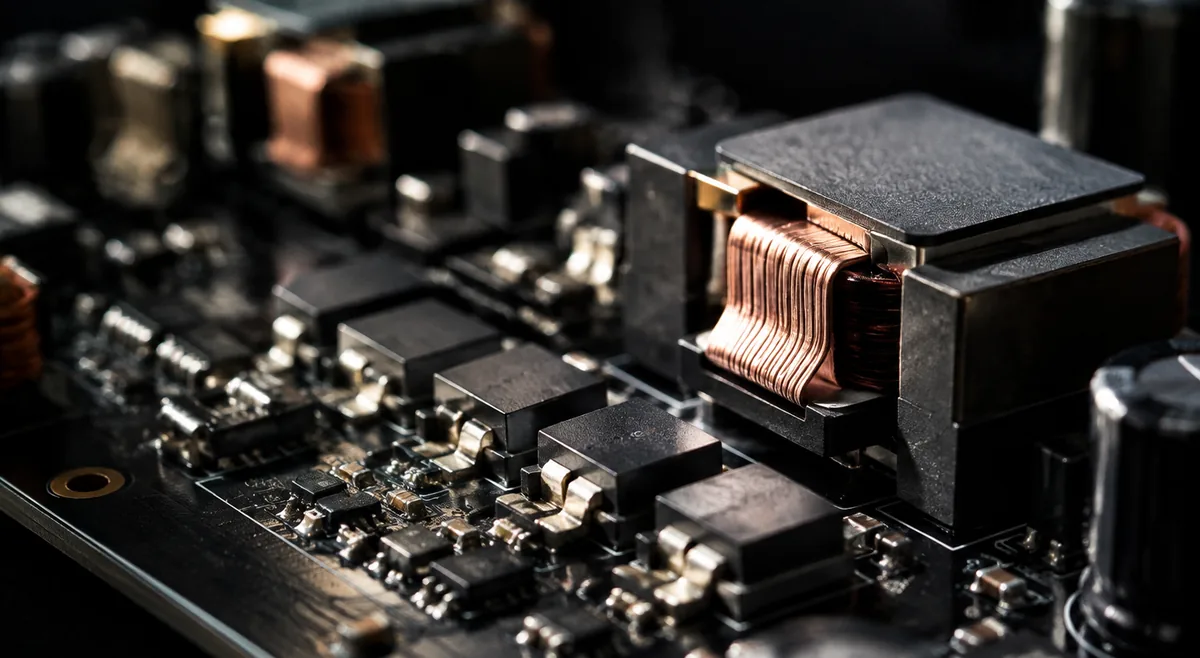
**The announcement (OFFICIAL — joint press release via GlobeNewswire, October 5, 2026).** Navitas Semiconductor (Nasdaq: NVTS) and Microchip Technology (Nasdaq: MCHP) collaborated on an **800V DC-to-6V DC reference design** — a power delivery board (PDB) for AI data-center rack power — comprising a reference board, software, and supporting documentation. It will be showcased at Microchip's OCP event during the **2026 OCP Global Summit, October 12–15, San Jose, California**. **Building blocks (OFFICIAL — named in the release).** Microchip **dsPIC33AK** digital signal controllers (200 MHz 32-bit core, double-precision FPU, 78 ps high-resolution PWMs, 12-bit ADCs up to 40 MSPS, library support for CNSA Suite 2.0 post-quantum cryptography; named family **dsPIC33AK256MPS306**); Microchip **TA100 CryptoAuthentication** device (secure boot, code authentication, MAC generation, trusted firmware updates, TLS root-of-trust operations); and **16× Navitas NV6034 GaNFast FETs (650 V, 17 mΩ)** in stacked half-bridge topology on the primary side, in DFN8×8 dual-side-cooled packages. Do not expect other part numbers to appear in this article — these are the only ones the release names. **Topology (OFFICIAL concept; detail MEDIA REPORTED).** Direct 800V-to-6V conversion **in one converter**, collapsing what would otherwise be an 800V→50V stage plus a 50V→6V stage. The 128:1 full-bridge LLC topology with planar transformers is a media-reported detail (bitcoinversus.tech), not release text. **Performance figures — targets, NOT measured results (OFFICIAL wording).** The release states **targets** of up to **96% peak efficiency at full load**, **1 MHz** switching frequency, and **2,100 W/in³** power density — about 20% thinner than a mobile phone, designed for close integration with the GPU board. The **20 kW** converter figure comes from media reporting (bitcoinversus.tech), not the press release. Presenting any of these as measured specifications would be fabrication. **Why 800V DC (MEDIA REPORTED industry context).** Google, Microsoft, and NVIDIA are working through the Open Compute Project to establish **800V DC as an open standard** for next-generation high-density AI data centers, with 80+ equipment and infrastructure companies in the ecosystem (Network World, ~August 2026; channelinsider). AWS has notably not committed. The physics is straightforward: P = V × I, so higher distribution voltage means lower current, and conductor losses scale with I²R — less copper, less heat, fewer conversion stages. Advocacy figures from the standards push claim 50–80% copper reduction, 8–12% annual energy OpEx reduction, and $4–8M CapEx savings per 10 MW build — treat these as reported claims from an interested party, not independent measurement. **Migration path (MEDIA REPORTED).** Near-term: **sidecar/side-power-rack** architectures converting existing AC to 800V DC near the compute racks (OCP "Diablo" spec, co-authored by Google/Meta/Microsoft: 100 kW–1 MW racks at ±400 VDC or 800 VDC) — existing AC switchgear and UPS need not be ripped out first. Longer-term: medium-voltage AC converted directly to an 800V DC backbone. Adjacent evidence the transition is broadening: Trane is testing a 3.5 MW 800V DC chiller, so cooling is converging on the same voltage architecture.
Why this design matters for component buyers
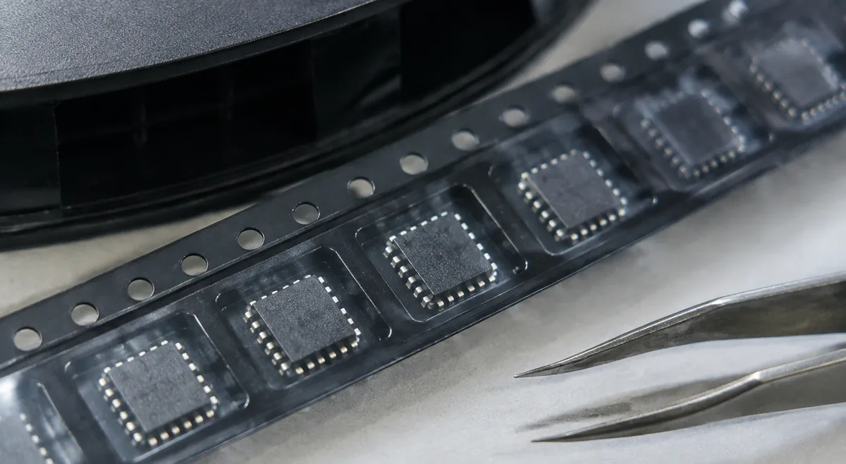
**GaN is moving from "emerging" to "designed-in" for AI power.** A joint reference design from a broadline power/MCU vendor plus a GaN pure-play, aligned to an OCP standard backed by three hyperscalers, is a demand signal for 650V-class GaN FETs. The 2,100 W/in³ density target is a GaN-enabled figure — silicon superjunction MOSFETs at 800V-class operation switch slower and need larger magnetics and cooling. Procurement teams buying power stages for AI servers should start qualifying GaN sources now: lead times and allocation tighten when a standard tips, and this is the window before it does. **The architecture bet to evaluate: single-stage vs two-stage.** This design collapses two conversion stages into one — fewer stages means higher end-to-end efficiency, but a harder design problem (128:1 LLC). When evaluating rack power vendors, ask whether their 800V path is single- or two-stage, and insist on **measured** efficiency, not target efficiency. A vendor quoting this reference design's 96% target as their product spec is selling you a PowerPoint. **Security is becoming a power-supply line item.** The TA100 root-of-trust device in a *power* reference design is the tell: hyperscaler supply-chain security requirements are migrating into power infrastructure. Expect secure-boot and firmware-authentication requirements to start appearing in PSU specifications. Budget not just for the IC, but for the key-management and secure-manufacturing overhead that comes with it. **It concentrates demand in specific component categories.** If 800V rack architectures ramp, component demand pools in: 650V-class GaN FETs (16 per board in this design), high-resolution digital power controllers (dsPIC33AK-class DSCs), high-speed current sensing, planar/low-profile magnetics, and hardware security ICs. That is a sourcing map, not a forecast — but it is where to aim qualification effort. **The OCP Global Summit (Oct 12–15) is the next data point.** Spec releases and workstream updates from the summit will show whether the 800V timeline is accelerating. Near-term, the sidecar architecture is the 2026–2027 reality; the MV-AC-to-800V backbone is the longer-term play.

A buyer checklist for AI rack power
**1. Ask single-stage or two-stage — and demand measured numbers.** Any 800V power vendor should be able to state their architecture and show measured efficiency curves. Targets are not specifications; this reference design's figures are explicitly targets. **2. Qualify 650V GaN sources now, before the standard tips.** The GaN second-source landscape includes Infineon (with GaN Systems), TI, EPC, Power Integrations, STMicroelectronics, Nexperia, and Renesas/Transphorm (general market context — verify pin, package, and driver compatibility per datasheet; none is presented here as a drop-in for any named part). Start the 6–12 month qualification cycle while allocation is still comfortable. **3. Put security ICs in the PSU BOM budget.** If your customers are hyperscalers or their supply chains, root-of-trust requirements will reach your power designs. Price the TA100-class device plus the provisioning infrastructure now, not as a surprise line item later. **4. Design for the migration path, not just the endpoint.** Sidecar 800V architectures that reuse existing AC infrastructure are the near-term deployment model. Power components and system designs that only make sense in a full 800V-backbone world are early — match your bets to the 2026–2027 sidecar reality. **5. Don't over-read one reference design.** It proves the building blocks are feasible; it does not prove deployment volume. The 800V ecosystem still needs the full chain — rectifiers, busbars, protection, safety certification — before racks ship at scale. One board is a signal, not a market.
The honest caveats
**96%, 1 MHz, 2,100 W/in³ are targets.** The release says so explicitly. Any article, vendor, or distributor presenting them as measured results is misreading the source. **No hyperscaler has adopted this design.** The OCP alignment is to the 800V DC *standard*, backed by Google/Microsoft/NVIDIA — not to this specific board. Conflating the two is the most common way this story gets overstated. **The economics figures are advocacy.** 50–80% copper reduction and the CapEx/OpEx savings come from the standards push's own materials. Directionally plausible given the physics; not independently verified. **GaN is not automatically the answer for every power stage.** At lower voltages and powers, silicon remains cost-competitive; GaN's advantage concentrates where switching frequency and density matter most — exactly this 800V-to-low-voltage, high-density application. Select per stage, not per trend.
Frequently asked questions
**Is the Microchip-Navitas 800V board a product I can buy?** No. It is a reference design — board, software, and documentation as an evaluation platform. There is no purchasable SKU, no datasheet spec, and no announced pricing or lead time. **What parts does it actually use?** Per the release: Microchip dsPIC33AK DSCs (dsPIC33AK256MPS306 family), Microchip TA100 CryptoAuthentication, and 16× Navitas NV6034 650V/17mΩ GaN FETs. Those are the only part numbers officially named. **Does 800V DC replace the 48V/54V rack bus?** It is the proposed next step up (OCP Open Rack V3 uses a 48V DC busbar; Eaton ships a 50V system). Near-term deployment is via sidecar architectures alongside existing infrastructure, not a forklift replacement. **When will 800V racks ship at scale?** No vendor has announced volume timelines tied to this design. Watch the OCP Global Summit (Oct 12–15, 2026) for spec and workstream updates — those are the next concrete timeline signals. **Should I switch my power designs to GaN now?** If you are designing AI-server or high-density power stages for 2026–2028 production, start GaN qualification now — the standards momentum plus this reference design make allocation tightening plausible. For lower-voltage, cost-sensitive stages, silicon remains the rational default. --- *This article is for informational purposes only and does not constitute investment or procurement advice. Announcement facts are from the companies' joint press release (Oct 5, 2026); industry context is media-reported and graded; performance figures are the release's stated targets, not measured results. Verify part-specific decisions against manufacturer datasheets and your authorized distributor.* --- --- ---
Manufacturer references
Use the latest guidance for the exact part and manufacturer when deciding acceptance criteria.